
8051 microcontroller is designed by
Intel in 1981. It is an 8-bit microcontroller. It is built with 40 pins DIP (dual inline package),
4kb of ROM storage and 128 bytes of RAM storage, 2 16-bit timers. It consists of are four parallel 8-bit ports,
which are programmable as well as addressable as per the requirement. An on-chip crystal
oscillator is integrated in the microcontroller having crystal frequency of 12 MHz.
The 8051 memory is organized in a
Harvard Architecture. Both the code memory space and data memory space begin at location 0x00 for internal or
external memory which is different from
the Princeton Architecture where code and data share same memory space. The advantage of the Harvard Architecture is not only doubling the memory
capacity of the microcontroller with same number of address lines but also
increases the reliability of the microcontroller, since there are no instructions to write to the code memory which is read only.
1. Features of 8051 Microcontroller
An 8051 microcontroller comes bundled with the following
features.
· 64K bytes on-chip
program memory (ROM)
· 128 bytes on-chip data memory (RAM)
· Four register
banks
· 128 user defined software
flags
· 8-bit bidirectional data bus
· 16-bit unidirectional address bus
· 32 general
purpose registers each of 8-bit
· 16 bit Timers (usually
2, but may have more or less)
· Three internal
and two external Interrupts
· Four 8-bit ports,(short model
have two 8-bit ports)
· 16-bit program
counter and data pointer
2. Architecture Of 8051 Microcontroller

8051 microcontroller has an internal program of 4K size and if needed an external memory can be added (by interfacing) of
size 60K maximum. So in total 64K size memory is available for 8051 micro controller. By default,
the External Access (EA) pin should be connected
Vcc so that instructions are fetched from internal memory initially. When the
limit of internal memory (4K) is
crossed, control will automatically move to external memory to fetch remaining instructions. If the programmer
wants to fetch instruction from external memory only (bypassing the internal memory), then he must connect External
Access (EA) pin to ground (GND).
2.2 Timers and Counters
Timer means which can give the delay
of particular time between some events. For example on or off the lights after every 2 sec. This delay can
be provided through some assembly
program but in microcontroller two hardware pins are
available for delay generation. These hardware
pins can be also used for counting some external events. How much times a number
is repeated in the given table is calculated by the counter.
In MC8051, two timer pins are
available T0 and T1, by these timers we can give the delay of particular time if we use these in timer mode. We can count external pulses at these pins if we use these pins in counter mode. 16 bits timers are available. Means we can
generate delay between 0000H to
FFFFH. Two special function registers
are available. If we want to load T0 with 16 bit data then we can load
separate lower 8 bit in TL0 and higher 8 bit in TH0. In the same way
for T1. TMOD, TCON registers
are used for controlling
timer operation.
2.3 Serial Port
There are two pins available for
serial communication TXD and RXD. Normally TXD is used for transmitting serial data which is in SBUF register, RXD is
used for receiving the serial data. SCON
register is used for controlling the operation.
2.4 Input Output
Ports
There are four input output ports
available P0, P1, P2, P3. Each port is 8 bit wide and has special function register P0, P1, P2, P3
which are bit addressable means each bit can be set or reset by the Bit instructions (SETB for high, CLR for low)
independently. The data at any port which is transmitting or receiving is in
these registers. The port 0 can
perform dual works. It is also used
as Lower order address bus (A0 to A7) multiplexed with 8 bit data bus P0.0 to
P0.7 is AD0 to AD7 respectively the
address bus and data bus is
demultiplex by the ALE signal and latch
which is further discussed in details. Port 2 can be used as I/O port as well
as higher order address bus A8 to
A15. Port 3 also have dual functions
it can be worked as I/O as well as each pin
of P3 has specific function. P3.0 – RXD – {Serial I / P for Asynchronous
communication Serial O / P for
synchronous communication. P3.1 – TXD – Serial data transmit. P3.2 – INT0 – External Interrupt 0. P3.3 – INT1 –
External Interrupt 1. P3.4 – T0 – Clock input for counter 0. P3.5 – T1 – Clock input for counter 1. P3.6 – WR – Signal for writing to external
memory. P3.7
– RD – Signal for reading from external memory.
When external memory
is interfaced with 8051 then P0 and P2 can’t be worked as I/O
port they works as address bus and data bus, otherwise they can be accessed as I/O ports.
2.5 Oscillator
It
is used for providing the clock to MC8051 which decides the speed or baud
rate of MC. We
use crystal which frequency vary from 4MHz to 30 MHz, normally we use 11.0592
MHz frequency.
2.6 Interrupts
Interrupts are defined as requests
because they can be refused (masked) if they are not used, that is when an interrupt is acknowledged. A special set
of events or routines are followed to
handle the interrupts. These special routines are known as interrupt handler or
interrupt service routines (ISR).
These are located at a special location in memory. • INT0 and INT1 are the pins for external interrupts.
3. Pin Diagram Of 8051 microcontroller
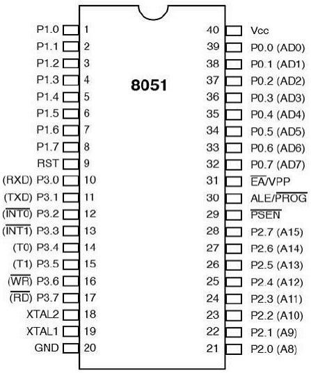
3.1
Pin Description
The EA' (External Access) pin is used
to control the internal or external memory access. The signal 0 is for external memory access and signal 1 for internal memory access. The PSEN' (Program Store Enable) is for reading external code memory when it is low (0) and EA
is also 0. The ALE (Address Latch Enable) activates the port 0 joined with port 2 to provide 16 bit external address bus to access the external memory. The ALE multiplexes the P0: 1 for latching address on P0 as A0-A7 in the 16 bit address buss, 0 for latching P0 as data I/O. P0.x is named ADx because P0 is multiplexed for Address bus and Data bus at different clock time. WR' provides the signal to write external data memory RD' provides the signal to read external data and code memory.
· PORT P1 (Pins 1 to 8): The port P1 is a port dedicated for general I/O purpose. The other ports P0, P2 and P3 have dual roles in addition to their basic I/O function.
• PORT P0 (pins 32 to 39): When the external memory access is required then Port P0 is multiplexed for address bus and data bus that can be used to access external memory in conjunction with port P2. P0 acts as A0-A7 in address bus and D0-D7 for port data. It can be used for general purpose I/O if no external memory presents.
• PORT P2 (pins 21 to 28): Similar to P0, the port P2 can also play a role (A8-A15) in the address bus in conjunction with PORT P0 to access external memory.
· PORT P3 (Pins 10 to 17): In addition to acting as a normal I/O port,
Ø P3.0 can be used for serial receive input pin(RXD) • P3.1 can be used for serial
transmit output pin(TXD) in a serial port,
Ø P3.2 and P3.3 can be used as external interrupt pins(INT0’ and INT1’),
Ø P3.4 and P3.5 are used for external counter input pins(T0 and T1),
Ø P3.6 and P3.7 can be used as external data memory write and read control signal
pins(WR’ and RD’)read and write pins for memory access.


0 Comments